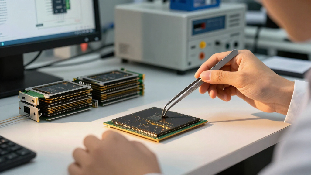
🔍 Read the full analysis: What Makes Up An AI Chip? Dies, Memory Stacks And Packaging on ThorstenMeyerAI.com

Prime made for students and young adults
- Fast, free delivery for dorm and study essentials
- Prime Video and Amazon Music included
- Member-only deals
TL;DR
Modern AI accelerators combine multiple compute dies, high-bandwidth memory stacks and a silicon interposer inside one package; the package is only one part of a much larger rack system. The source explainer says memory bandwidth and advanced packaging are important constraints, but some specifications and supply forecasts come from company statements and remain subject to change.
A November 22 explainer from ThorstenMeyerAI.com describes how modern AI accelerators are built from compute dies, stacked high-bandwidth memory and advanced packaging, rather than a single piece of silicon. The account matters because the hardware’s performance depends not only on its processors, but also on moving data to them and manufacturing the complex packages that connect the components.
The explainer uses Nvidia and AMD products to show how an accelerator package brings together several layers. At the bottom, a package substrate carries power and signals to the module. Above it, a silicon interposer provides dense connections between compute dies and memory stacks. The source says its own 3D models use the reported layer order and component counts, but schematic sizes: neither company publishes the dimensions needed to model the parts to scale.
High-bandwidth memory, or HBM, is made from DRAM chips stacked vertically and joined by through-silicon vias. This places memory close to the compute dies and allows many connections between them. The source cites Nvidia’s product information for a stated 19.2 terabytes per second of memory bandwidth for Rubin, compared with 900 gigabytes per second for V100. Those figures refer to different generations of Nvidia GPU and are presented as product specifications.
The package is part of a larger system. The source describes Nvidia’s GB200 and GB300 NVL72 racks as containing 72 GPUs and 36 CPUs, arranged across compute trays, switch trays and power equipment. Nvidia’s documentation describes liquid cooling through cold plates attached to processors; the source gives a cooling capacity of 120 kilowatts for a GB200 NVL72 rack. These figures are tied to the named systems, not all AI servers.
Why Packaging Shapes AI Capacity
AI performance is often discussed in terms of processor speed, but data movement and memory bandwidth also affect how much work a system can complete. If processors cannot receive data quickly enough, adding compute capacity alone may not produce a matching increase in useful throughput. That is why memory stacks and the connections between them and the compute dies are central parts of accelerator design.
Packaging also affects how many accelerators can be produced. The source identifies advanced interposers and the assembly of multiple dies and HBM stacks as manufacturing constraints. It reports that SK hynix expects demand for memory to exceed supply through 2030; that is the company’s forecast, not a verified guarantee about future supply. If constraints persist, businesses could face limits on deployment or higher costs, though the explainer does not quantify either outcome.
Finally, a rack-level view shows why a chip specification does not describe the full infrastructure requirement. A dense rack includes networking, power delivery and liquid cooling alongside accelerators. Buyers evaluating AI capacity must account for the whole system, including the facility’s ability to power and cool it.
Popular right now

De'Longhi Classic Signature Espresso Machine with Adjustable Milk Frother

Samsung 55-Inch M70H Series 4K HDR Mini-LED Smart TV with HDMI Cable and 12-Month CPS Warranty

KitchenAid Artisan 5-Quart Tilt-Head Stand Mixer, Milkshake
As an affiliate, we earn on qualifying purchases.
From Silicon Dies to HBM Towers
Manufacturing equipment can print only up to a limited area in one exposure, called a reticle. The source says TSMC’s CoWoS-S packaging can accommodate an interposer up to about 2,700 square millimetres, or 3.3 times reticle size, according to TSMC. For larger designs, CoWoS-L connects smaller silicon bridges in a carrier layer. The source reports TSMC’s CEO said on October 15, 2026, that the company was in production of five-times-reticle-size designs and working on larger formats. Those statements describe the company’s packaging technology and production status.
The compute designs cited show different ways to combine silicon. Nvidia’s Rubin GPU is described by the company as having two reticle-limited compute dies and 336 billion transistors. AMD says its MI350 Series integrates eight vertically stacked accelerator complex dies and two I/O dies; its MI355X has 185 billion transistors. The source also says AMD lists MI450X and MI455X as using CoWoS-L packaging, while its next-generation designs use stacked 3D hybrid-bonded compute dies.
HBM stacks are also changing. The source cites JEDEC’s April 2025 HBM4 standard, which allows stacks of four, eight, 12 or 16 layers and up to 64 gigabytes per stack. SK hynix and Samsung have separately described advances in thinner or more closely spaced memory layers. These company statements and standards describe design capabilities; they do not mean every accelerator uses the maximum stack height or capacity.
“The company expects demand to exceed supply “through 2030.””
— SK hynix, as reported by ThorstenMeyerAI.com
Limits of the Published Specifications
Some figures are vendor specifications or forecasts, rather than independently verified measures of performance or supply. In particular, the expectation that memory demand will exceed supply through 2030 is attributed to SK hynix. The source does not provide an independent market forecast or quantify how shortages could affect prices, delivery times or AI deployments.
The source says its 3D models are schematic because exact package, die and memory-stack dimensions are not published by Nvidia or AMD. Product configurations can also vary by system and generation. The explainer does not establish how widely each named package is shipping, how many units manufacturers can produce, or whether every listed rack configuration is available to customers on the same terms.
Production and Rack Deployments
The next developments to watch are packaging capacity, HBM supply and product availability as manufacturers bring larger and more complex accelerator designs to market. The source says TSMC is working on interposer formats beyond five times reticle size, while citing the company’s reported progress as of October 15, 2026; it gives no timetable for the nine- and 14-times formats.
For buyers, the practical next step is to compare complete server configurations rather than GPU names alone: memory capacity and bandwidth, power requirements, cooling, networking and delivery schedules all affect usable capacity. The source identifies the Vera Rubin NVL72 as listed by Nvidia as available, but does not provide independent shipment data or clarify deployment volumes. Those details will be needed to establish how quickly announced hardware translates into installed AI capacity.
Key Questions
What components make up an AI accelerator package?
A package can include compute dies, HBM stacks, a silicon interposer and a package substrate. The substrate carries power and signals to the module, while the interposer provides dense connections between the compute and memory components.
What does HBM mean?
HBM stands for high-bandwidth memory. It uses DRAM chips stacked vertically and connected with through-silicon vias, placing memory close to accelerator compute dies.
Why does packaging matter for AI hardware?
Packaging connects multiple dies and memory stacks with many short, dense connections. It can affect data movement, performance and manufacturing capacity, though the source does not quantify how much each factor limits current deployments.
How many GPUs are in an Nvidia NVL72 rack?
The source describes the GB200 and GB300 NVL72 configurations as having 72 GPUs and 36 CPUs per rack, alongside networking and power equipment. The figure applies to those named rack systems.
Is a shortage of HBM guaranteed through 2030?
No. The source attributes that outlook to SK hynix’s forecast that demand will exceed supply through 2030. It is a company expectation, not a confirmed account of future supply.
Source: ThorstenMeyerAI.com